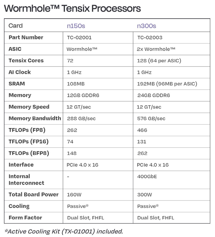
Back in part 4, we were considering the entire Wormhole PCIe card, and then in part 5 we zoomed in on a single T tile. Today I'm going to zoom in even more, looking at the box that part 5 labelled "Tensix Vector (SFPU)". To draw a very rough analogy to GPU graphics programming, Tensix Unpack/Matrix/Pack are somewhat like a (configurable) fixed-function pipeline, whereas Tensix Vector can execute arbitrary shader programs. To instead draw a very rough analogy to GPU AI programming, Tensix Unpack/Matrix/Pack are like tensor cores, whereas Tensix Vector is like CUDA cores. That said, neither analogy is entirely accurate, as fundamentally this hardware is trying to be its own thing rather than trying to be a GPU. Continuing the AI theme, Unpack/Matrix/Pack can execute (amongst other things) linear layers consisting of matrix multiplication, optionally adding a bias, and then optionally ReLU, but once you stray too much beyond this, you'll need to pull in Tensix Vector. Tanh? Tensix Vector. Dropout? Tensix Vector. Cumsum? You guessed it, Tensix Vector.
The Tenstorrent documentation and code often refer to Tensix Vector as "SFPU", but I'll stick to calling it Tensix Vector. The hardware is wrapped with an API/toolchain/compiler called SFPI, which has an associated documentation page. I'll try to explain the raw underlying hardware, though I'll occasionally make reference to things the SFPI toolchain does. The documentation makes reference to an emulator in main.cc, which I can't find per se, but sfpu.cc gets somewhat close. Unfortunately, it operates at the level of a partially-lowered compiler IR, so some interpretation is required to map between that IR and actual machine instructions. Speaking of machine instructions, we saw the general layout of Tensix instructions in part 5. As a reminder, these are disjoint from RISC-V instructions, so there's no relation between the RISC-V "V" (for Vector) extension and Tensix Vector, and the general instruction layout is:

Whereas RISC-V "V" tries to present arbitrary-length vectors, Tensix Vector is a good old SIMD instruction set, like AArch64 NEON or x86 SSE/AVX, with 32 SIMD lanes in Wormhole. Each lane consists of 32 bits, which depending on the instruction are viewed as either fp32 or int32 or signmag32.
With the introduction done, we can start to get into the details. The remainder of this post gets very low-level and very dense, so skip it if that's not for you.
Execution environment
Before diving into the Tensix Vector instructions, it is useful to consider the environment in which the instructions execute. The important parts are:
| Size |
|---|
Vector registers (L0-L7) | 8 registers, 32 lanes per register, 32b per lane |
|---|
| Fixed constants | 4 values, 32b each |
|---|
| Programmable constants | 4 "constants", 8 lanes per constant, 32b per lane |
|---|
| Flags active | 1b |
|---|
| Per lane flags | 32 lanes, 1b per lane |
|---|
| Flag stack | Between 0 and 8 entries, (1+32×1)b per entry |
|---|
| PRNG | 32 lanes, 32b LFSR per lane (with caveats) |
|---|
Dst | Either 512 rows, 16 lanes per row, 32b per lane
Or 1024 rows, 16 lanes per row, 16b per lane |
|---|
RWC_Dst | 10b |
|---|
The vector registers are called L0 through L7, which is a somewhat poor choice of naming scheme, given that L1 could easily instead refer to the 1464 KiB of SRAM on each tile. Considering the vector registers and the constants all together, there are 16 possible operands, which are encoded into 4b fields in instructions like so:
| Encoding | Meaning |
|---|
0 - 7 | Vector Registers L0 - L7 |
8 | Fixed Constant 0.8373 (bit pattern 0x3F56594B) |
9 | Fixed Constant 0.0 (bit pattern 0x00000000) |
10 | Fixed Constant 1.0 (bit pattern 0x3F800000) |
11 | Programmable constant, though toolchain requires it to be -1.0 |
12 | Programmable constant (vConstIntPrgm0 / vConstFloatPrgm0) |
13 | Programmable constant (vConstIntPrgm1 / vConstFloatPrgm1) |
14 | Programmable constant (vConstIntPrgm2 / vConstFloatPrgm2) |
15 | Fixed Constant lane_number << 1 (i.e. 0, 2, 4, ..., 62) |
The programmable constants are set using the SFPCONFIG instruction, which we'll cover later. The toolchain exposes two names for each, differing in type, but they're backed by the same storage. The programmable constants usually have the same value in all eight of their lanes, but in the event that the lanes end up with different values, four copies of the constant are stacked horizontally to form 32 lanes. The fixed constants 0.8373 and 0.0 and 1.0 have the same value in every lane, and then the final fixed constant has a different value in every lane.
Next up are flags. Flags can be active or inactive. If flags are active, then there is a 1b flag per lane controlling whether that lane is enabled. Initially all lanes are enabled, and then various instructions can "refine" the per-lane flag: lanes which fail the condition switch from enabled to disabled (whilst previously disabled lanes remain disabled, with neither their contents nor their flags being updated). The toolchain exposes refinement through the v_and macro. If flags are inactive, then all lanes are enabled regardless of the 1b flag per lane. There is also a stack on to which all this state can be pushed and then later popped. Contrast this to Apple G13: there each lane has a disabled counter rather than a stack of flags.
We then find some PRNG state, which can optionally be used for stochastic rounding. The seeding mechanism leaves something to be desired though, as does the state update function, so I'd recommend avoiding the PRNG if you care your random numbers having high quality and low correlation.
The final notable part of the execution environment is Dst: the large 2D piece of memory that the Tensix Matrix unit writes the result of matrix operations to. The rows of this memory are 16 scalars wide, the combination of 16 rows is typically called a 16x16 face (which is what a lot of the LLK code operates on), and then the combination of four such faces is typically called a 32x32 tile (which is what the TT-Metal API exposes). Expressed differently, 64 rows of Dst are required for holding a 32x32 tile. The SFPLOAD and SFPSTORE instructions transfer data between a single vector register and some rows of Dst (they do not transfer between a vector register and main memory!), with the target rows determined by the summation of an immediate operand to SFPLOAD / SFPSTORE and the RWC_Dst variable, taken modulo the number of rows of Dst (512 when it is holding 32b scalars, 1024 when holding 16b scalars). The toolchain exposes RWC_Dst via the slightly questionable syntax dst_reg++.
Notation
I'll use VD to mean an arbitrary vector register used as the output (and often also an input) of an instruction. I'll use VA / VB / VC to mean arbitrary vector registers or constants used as inputs to an instruction. When instructions operate on fixed registers, I'll use the names L0 through L7. Scalar inputs that come from N bits within the instruction itself are referred to as ImmN. Signed immediates (in two's complement form) of N+1 bits will be ±ImmN, the range of which is -(2N) through (+2N)-1.
Some instructions can operate in several distinct modes, in which case they'll be listed multiple times in different sections and marked with (‡) each time.
Instruction encoding
The Mod0 family of encodings put a "VD" field at the top, then a modifier field, then immediates at the bottom:


Meanwhile, the Mod1 family of encodings put a modifier field at the bottom, then "VD", then other operands, then immediates at the top:


Each instruction links through to emulation code for that instruction, giving (my best guess of) its precise encoding and behaviour. In each case, the encoding will be one of the above, but the opcode varies by instruction, as does the interpretation of Mod0 / Mod1.
With the stage set, we can now take a brief look at all the instructions handled by Tensix Vector.
Int32 arithmetic and bitwise operations
We begin with some gentle integer instructions:
| Per-lane behaviour (int32) |
|---|
SFPIADD | VD = VC ± VD or VD = VC ± Imm11
Optionally refine flags based on VD < 0 or inverse thereof |
|---|
SFPAND | VD &= VC |
|---|
SFPOR | VD |= VC |
|---|
SFPXOR | VD ^= VC |
|---|
SFPNOT | VD = ~VC |
|---|
SFPLZ | VD = CountLeadingZeros(VC)
Optionally refine flags based on VC != 0 or inverse thereof |
|---|
SFPABS (‡) | VD = Abs(VC) |
|---|
SFPSHFT | VD = VD << (VC % 32) or VD = VD >> (-VC % 32) or
VD = VD << Imm5 or VD = VD >> -Imm5 |
|---|
SFPSHFT2 (‡) | VD = VB << (VC % 32) or VD = VB >> (-VC % 32) |
|---|
SFPSETCC | Refine flags based on VC != 0 or VC < 0 or inverse of either |
|---|
Nothing greatly surprising here, though it is a shame that so many instructions treat VD as both an input and an output (this isn't for lack of encoding space, as there's plently of that, and isn't for lack of register file ports, as SFPMAD requires three read ports and a write port, so I'm not sure of the rationale here). Shifts are all done modulo 32, with the sign of the shift amount determining whether the shift is left or right. Right shifts are always unsigned, though apparently Blackhole adds support for signed right shifts. There's also a somewhat insane variant of SFPSHFT2 that shifts VB by an immediate, but bits 12 through 15 specify both VB and (part of) the immediate, so the possible options there are L0 << 0, L1 << 1, L2 << 2, and so forth.
Flags are generally refined based on the sign or the zero-ness of the result. The conditions VC != 0 and VC < 0 are native, as are their inverses VC == 0 and VC >= 0. The non-native VC > 0 is achieved by refining on VC >= 0 and then refining on VC != 0. Its inverse (VC <= 0) is achieved by refining on VC >= 0 and then refining on VC != 0 and then issuing SFPCOMPC to invert the overall result. Three instructions for VC <= 0 isn't great, but again is addressed in Blackhole. Comparisons where the right hand side isn't zero are done by subtracting the two operands, and then comparing the subtraction result against zero. This causes < / <= / > / >= to do the wrong thing if overflow occurs during the subtraction, which is mildly concerning.
Flag stack
| Per-lane behaviour |
|---|
SFPENCC | Configure whether flags are active, also set flags |
|---|
SFPPUSHC | Push copy of flags on to flag stack |
|---|
SFPCOMPC | Invert per-lane flags, using top of stack as context |
|---|
SFPPOPC | Pop from flag stack into flags, or read top of stack into flags |
|---|
The SFPENCC instruction is used to initialise the flags subsystem: it can set flags to active, and initialise the per-lane flags to either enable or disable all lanes.
SFPPUSHC and SFPPOPC mostly do what you'd expect. If SFPPUSHC is used more than eight times, then it'll start overwriting previous entries. The stack size counter is four bits, and it too will wrap if SFPPUSHC is used sixteen times. If SFPPOPC is used with the size counter equal to zero, then the counter will underflow to fiveteen, but the resultant flags state will always be all lanes active. I would not advise trying to do anything clever with stack underflow or overflow.
SFPCOMPC is slightly interesting: it inverts the per-lane flags, but does this subject to the the state on the top of the stack; lanes that would be disabled in that state are set to disabled rather than being inverted.
Fp32 field manipulation
Up next are some unconventional, though not unwelcome, instructions to manipulate the three fields of an IEEE754 float:
| Per-lane behaviour (fp32 sign/exponent/mantissa) |
|---|
SFPEXEXP | VD = VC.Exponent or VD = VC.Exponent - 127
Optionally refine flags based on VD < 0 or inverse thereof |
|---|
SFPEXMAN | VD = { 0, !Imm1, VC.Mantissa} |
|---|
SFPMOV (‡) | VD = {!VC.Sign, VC.Exponent, VC.Mantissa} |
|---|
SFPSETSGN | VD = { VD.Sign, VC.Exponent, VC.Mantissa} or
VD = { Imm1, VC.Exponent, VC.Mantissa} |
|---|
SFPABS (‡) | VD = { 0, VC.Exponent, VC.Mantissa} |
|---|
SFPSETEXP | VD = { VC.Sign, VD.Mantissa & 255, VC.Mantissa} or
VD = { VC.Sign, VD.Exponent, VC.Mantissa} or
VD = { VC.Sign, Imm8, VC.Mantissa} |
|---|
SFPSETMAN | VD = { VC.Sign, VC.Exponent, VD.Mantissa} or
VD = { VC.Sign, VC.Exponent, Imm12 << 11} |
|---|
SFPDIVP2 | VD = { VC.Sign, Imm8, VC.Mantissa} or
VD = { VC.Sign, VC.Exponent ± Imm7, VC.Mantissa} |
|---|
There is no SFPEXSGN instruction, as integer instructions suffice for this: SFPSETCC can refine flags based on the sign bit, and SFPSHFT can do a right shift by 31 to extract just the sign bit.
The SFPDIVP2 instruction can perform addition/subtraction on the exponent field, thereby providing multiplication or division by a power of two, though the arithmetic will wrap around if it overflows, so some care is required. The only saving grace is that the VC.Exponent ± Imm7 form will leave VC untouched if it starts as ±Inf or ±NaN. If wrapping is a concern, use SFPMULI instead (described in the next section).
There is some overlap between instructions here; an absolute-value function can be built from SFPSETSGN, or SFPABS can be used for this. Similarly, one mode of SFPSETEXP is completely identical to one mode of SFPDIVP2.
Fp32 arithmetic
Then we reach the floating point multiply/add unit:
| Per-lane behaviour (fp32) |
|---|
SFPMUL | VD = VA * VB + 0 |
|---|
SFPADD | VD = 1 * VB + VC |
|---|
SFPMAD | VD = VA * VB + VC |
|---|
SFPMULI | VD *= Bf16ToFp32(Imm16) |
|---|
SFPADDI | VD += Bf16ToFp32(Imm16) |
|---|
SFPLUT | TmpA, TmpC = LUT({L0.Low16, L1.Low16, L2.Low16}, Abs(L3))
VD = TmpA * Abs(L3) + TmpC
|
|---|
SFPLUTFP32 | TmpA, TmpC = LUT({L0, L1, L2, L4, L5, L6}, Abs(L3))
VD = TmpA * Abs(L3) + TmpC
|
|---|
All of these instructions take two cycles, i.e. VD is not available until two cycles after the instruction is issued. An SFPNOP instruction must be inserted if the next instruction would otherwise want to consume VD (Blackhole relieves the compiler of this duty).
There is no fp32 subtract instruction; it is instead achieved by SFPMAD with VB set to -1.0. Most ISAs with a floating-point fused-multiply-add instruction have variants of the instruction to negate the result of the multiplication and/or the negate the addend, as doing so is incredibly cheap in hardware. This glaring omission is seemingly corrected in Blackhole.
The SFPADD instruction always has VA set to the constant 1.0 by the compiler, allowing hardware to treat SFPADD exactly like SFPMAD if it so desires. Similarly, SFPMUL always has VC set to the constant 0.0 by the compiler, allowing hardware to treat SFPMUL exactly like SFPMAD. The chip I'm playing with indeed treats SFPADD and SFPMUL exactly like SFPMAD, though future chips might be able to just add or just multiply faster than SFPMAD (e.g. Zen 4 takes four cycles for a multiply-add, but just 3 cycles for either a multiply or an add).
There are no dedicated fp32 comparison instructions (though see the min/max mode of SFPSWAP described later), as the integer SFPSETCC generally suffices, though this does mean that -NaN is considered less than -Inf and +Inf is considered less than +NaN. It would also mean that -0 is considered less than +0, but it looks like all arithmetic instructions normalize -0 to +0 (similarly, it looks like all denormal inputs are treated as zero and all denormal outputs are flushed to +0; see also Tenstorrent's statement on infinities and NaNs and denormals).
The unusual instructions are SFPLUT and SFPLUTFP32, which create a 3-element or 6-element table from various bits of L0/L1/L2 and optionally L4/L5/L6, then use the magnitude of L3 to determine which table element to use, extract TmpA and TmpC from said element, calculate VD = TmpA * Abs(L3) + TmpC, then optionally overwrite the sign of the result with the original sign of L3. These instructions allow for various unary functions to be approximated in a piecewise linear fashion (similar in spirit, though not at all in implementation, to genlut in Apple's AMX).
For SFPLUT, the table ranges are:
| TmpA (multiplicand) | TmpC (addend) |
|---|
Abs(L3) < 1.0 | Fp8ToFp32((L0 >> 8) & 255) | Fp8ToFp32(L0 & 255) |
|---|
1.0 ≤ Abs(L3) < 2.0 | Fp8ToFp32((L1 >> 8) & 255) | Fp8ToFp32(L1 & 255) |
|---|
2.0 ≤ Abs(L3) | Fp8ToFp32((L2 >> 8) & 255) | Fp8ToFp32(L2 & 255) |
|---|
Whereas for SFPLUTFP32 in mode FP16_3ENTRY_TABLE:
| TmpA (multiplicand) | TmpC (addend) |
|---|
Abs(L3) < 1.0 | Fp16ToFp32(L0 >> 16) | Fp16ToFp32(L0 & 0xffff) |
|---|
1.0 ≤ Abs(L3) < 2.0 | Fp16ToFp32(L1 >> 16) | Fp16ToFp32(L1 & 0xffff) |
|---|
2.0 ≤ Abs(L3) | Fp16ToFp32(L2 >> 16) | Fp16ToFp32(L2 & 0xffff) |
|---|
For SFPLUTFP32 in mode FP32_3ENTRY_TABLE:
| TmpA (multiplicand) | TmpC (addend) |
|---|
Abs(L3) < 1.0 | L0 | L4 |
|---|
1.0 ≤ Abs(L3) < 2.0 | L1 | L5 |
|---|
2.0 ≤ Abs(L3) | L2 | L6 |
|---|
For SFPLUTFP32 in mode FP16_6ENTRY_TABLE1:
| TmpA (multiplicand) | TmpC (addend) |
|---|
Abs(L3) < 0.5 | Fp16ToFp32(L0 & 0xffff) | Fp16ToFp32(L4 & 0xffff) |
|---|
0.5 ≤ Abs(L3) < 1.0 | Fp16ToFp32(L0 >> 16) | Fp16ToFp32(L4 >> 16) |
|---|
1.0 ≤ Abs(L3) < 1.5 | Fp16ToFp32(L1 & 0xffff) | Fp16ToFp32(L5 & 0xffff) |
|---|
1.5 ≤ Abs(L3) < 2.0 | Fp16ToFp32(L1 >> 16) | Fp16ToFp32(L5 >> 16) |
|---|
2.0 ≤ Abs(L3) < 3.0 | Fp16ToFp32(L2 & 0xffff) | Fp16ToFp32(L6 & 0xffff) |
|---|
3.0 ≤ Abs(L3) | Fp16ToFp32(L2 >> 16) | Fp16ToFp32(L6 >> 16) |
|---|
And finally SFPLUTFP32 in mode FP16_6ENTRY_TABLE2:
| TmpA (multiplicand) | TmpC (addend) |
|---|
Abs(L3) < 0.5 | Fp16ToFp32(L0 & 0xffff) | Fp16ToFp32(L4 & 0xffff) |
|---|
0.5 ≤ Abs(L3) < 1.0 | Fp16ToFp32(L0 >> 16) | Fp16ToFp32(L4 >> 16) |
|---|
1.0 ≤ Abs(L3) < 1.5 | Fp16ToFp32(L1 & 0xffff) | Fp16ToFp32(L5 & 0xffff) |
|---|
1.5 ≤ Abs(L3) < 2.0 | Fp16ToFp32(L1 >> 16) | Fp16ToFp32(L5 >> 16) |
|---|
2.0 ≤ Abs(L3) < 4.0 | Fp16ToFp32(L2 & 0xffff) | Fp16ToFp32(L6 & 0xffff) |
|---|
4.0 ≤ Abs(L3) | Fp16ToFp32(L2 >> 16) | Fp16ToFp32(L6 >> 16) |
|---|
Many of the instructions in this section also support a mode whereby the result of the instruction isn't written to VD, but is instead written to the register number in the low four bits of L7. This can be viewed as a kind of scatter operation. SFPMAD also supports a kind of gather operation: rather than reading from VA, the multiplicand input can be taken from the register number in the low four bits of L7.
Min / max / swap
| Per-lane behaviour (fp32 or signmag32) |
|---|
SFPSWAP (‡) | VD, VC = Min(VD, VC), Max(VD, VC) |
|---|
SFPSWAP (‡) | VD, VC = VC, VD |
|---|
This instruction takes two cycles, possibly because it has two destinations and there's only one write port on the register file, and SFPSWAP must be followed by SFPNOP. When doing min / max, it uses the total ordering whereby -NaN < -Inf < finite negative values < -0 < +0 < finite positive values < +Inf < +NaN. The smaller of the two inputs ends up in VD, and the larger in VC. There are also variants which compute Min,Max for some groups of 8 lanes, and Max,Min for other groups of 8 lanes.
This is not an arithmetic instruction, so it does not flush denormals on input or on output. This means it can also be used for 32-bit integers in sign/magnitude form. The plain swap can also be used on int32 lanes.
Data type conversions to / from fp32
| Per-lane behaviour |
|---|
SFPSTOCHRND (‡) | VD = Fp32ToBf16(VC) << 16 |
|---|
SFPSTOCHRND (‡) | VD = Fp32ToTf32(VC) |
|---|
SFPSTOCHRND (‡) | VD = Fp32ToInt32(Min(Abs(VC), 255)) or
VD = Fp32ToInt32(Min(Abs(VC), 65535)) |
|---|
SFPSTOCHRND (‡) | VD = Fp32ToSignMag32(Clamp(VC, ±127)) or
VD = Fp32ToSignMag32(Clamp(VC, ±32767)) |
|---|
SFPCAST | VD = SignMag32ToFp32(VC) |
|---|
All of the above support two rounding modes, either stochastic rounding or round to nearest (SFPSTOCHRND resolves ties away from zero, SFPCAST resolves ties to even, which seems like a strange discrepancy). The stochastic rounding relies on the hardware PRNG, though as mentioned in the introduction, the quality of its randomness is poor: adjacent vector lanes will have 30 out of 32 bits in common, and consecutive random values within a lane will have 31 out of 32 bits in common. This leads to significant correlation between random values if more than one random value is obtained.
The PRNG state can also be observed directly with an oddball variant of SFPMOV:
| Per-lane behaviour |
|---|
SFPMOV (‡) | VD = RandomInt32() |
|---|
SFPNOP | No-op, delay subsequent instructions by one cycle |
|---|
SFPNOP is listed here as it is required for PRNG seeding: the seeding procedure involves writing the new seed to the PRNG_SEED::Seed_Val configuration register and then executing a bunch of SFPNOP instructions.
Rounding and clamping of sign / magnitude integers
| Per-lane behaviour (signmag32) |
|---|
SFPSTOCHRND (‡) | VD = Min(Round(Abs(VC) >> (VB % 32)), 255) or
VD = Min(Round(Abs(VC) >> Imm5), 255) |
|---|
SFPSTOCHRND (‡) | VD = Clamp(Round(VC >> (VB % 32)), ±127) or
VD = Clamp(Round(VC >> Imm5), ±127) |
|---|
All of the above support two rounding modes, based on the shifted-out bits: either stochastic rounding or round to nearest with ties away from zero. The toolchain uses the names int32_to_uint8 and int32_to_int8 for these operations. The PRNG used for stochastic rounding is the same as in the previous section.
Note that the lane type here is signmag32: the high bit is a sign bit, and then the low 31 bits are a magnitude. When the magnitude is clamped, it stays in the low bits. Negative zero is allowed as an input, but is always normalised to +0 on output.
Constants
| Per-lane behaviour |
|---|
SFPLOADI | VD = Bf16ToFp32(Imm16) or
VD = Fp16ToFp32(Imm16) or
VD = Imm16 or
VD = ±Imm15 or
VD.High16 = Imm16 or
VD.Low16 = Imm16 |
|---|
SFPCONFIG (‡) | SelectedProgrammableConstant = L0[0:8] |
|---|
There are various modes of SFPLOADI for setting all lanes of a vector register to a 16-bit immediate. A 32-bit immediate can be formed by using two SFPLOADI instructions: Bf16ToFp32 or High16 to set the high 16 bits, and then Low16 to set just the low 16 bits. A selection of interesting 32-bit values can also be formed in a single cycle by using SFPSETSGN / SFPDIVP2 / SFPSETMAN with VC set to one of the fixed constants.
To load a value into one of the programmable constants, first use SFPLOADI to load it into all lanes of L0, then use SFPCONFIG to copy L0[0:8] into one of the programmable constants.
Cross-lane data movement
| Whole-vector behaviour |
|---|
SFPMOV (‡) | VD = VC |
|---|
SFPSHFT2 (‡) | L0, L1, L2, L3 = L1, L2, L3, Zeros or
L0, L1, L2, L3 = L1, L2, L3, {L0[8:32], Zeros[0:8]} or
L0, L1, L2, L3 = L1, L2, L3, RotateLanesRight(VC) |
|---|
SFPSHFT2 (‡) | VD = RotateLanesRight(VC) or
VD = ShiftLanesRight(VC) |
|---|
SFPTRANSP | Transpose(L0, L1, L2, L3); Transpose(L4, L5, L6, L7) |
|---|
The RotateLanesRight function rotates each group of eight lanes right by one lane, so VD = RotateLanesRight(VC) does VD[i] = VC[i&7 ? i-1 : i+7]. The similar VD = ShiftLanesRight(VC) is meant to do VD[i] = i&7 ? VC[i-1] : 0, but a hardware bug means that instead of every 8th lane getting zero, it gets whatever the most recent RotateLanesRight wrote to that lane. Between this and the comedy mode that can do L0 << 0 or L1 << 1 or L2 << 2 etc, I get the impression that SFPSHFT2 was poorly specified and/or poorly tested. Hopefully it is all fixed in Blackhole.
The variants of SFPSHFT2 involving RotateLanesRight / ShiftLanesRight require two cycles to execute. If it weren't for this, the variant of SFPSHFT2 which moves zeros to L3 would be redundant, as it could be implemented with the RotateLanesRight variant with constant zero as VC.
Meanwhile, SFPTRANSP causes the following transformation:
| L0 | L1 | L2 | L3 |
|---|
[ 0: 8] | L0[0:8] | L0[8:16] | L0[16:24] | L0[24:32] |
|---|
[ 8:16] | L1[0:8] | L1[8:16] | L1[16:24] | L1[24:32] |
|---|
[16:24] | L2[0:8] | L2[8:16] | L2[16:24] | L2[24:32] |
|---|
[24:32] | L3[0:8] | L3[8:16] | L3[16:24] | L3[24:32] |
|---|
| L4 | L5 | L6 | L7 |
|---|
[ 0: 8] | L4[0:8] | L4[8:16] | L4[16:24] | L4[24:32] |
|---|
[ 8:16] | L5[0:8] | L5[8:16] | L5[16:24] | L5[24:32] |
|---|
[16:24] | L6[0:8] | L6[8:16] | L6[16:24] | L6[24:32] |
|---|
[24:32] | L7[0:8] | L7[8:16] | L7[16:24] | L7[24:32] |
|---|
The naïve implementation of this instruction would either require 8 cycles to execute, or require a register file with 8 write ports. Neither of these things seems likely, so perhaps what we're seeing is 8x 32b as the fundamental unit of storage, L0/L1/L2/L3 being backed by 16 units of storage, and the SFPTRANSP instruction flipping how L0/L1/L2/L3 map on to that storage (ditto L4/L5/L6/L7, and their backing 16 units of storage). The modes of SFPSHFT2 which write to all four of L0 through L3 might pull a similar trick; actually writing to one register and just shuffling indices for the others.
Transfer between Dst and vector registers
At long last, we reach the means of getting data in and out of the vector world:
| Whole-vector behaviour |
|---|
SFPLOAD | VD = Dst[R:R+4, 0:15:2] or VD = Dst[R:R+4, 1:16:2] |
|---|
SFPSTORE | Dst[R:R+4, 0:15:2] = VD or Dst[R:R+4, 1:16:2] = VD |
|---|
Given that rows of Dst have 16 lanes, and vector registers have 32 lanes, you might expect SFPLOAD / SFPSTORE to reference two rows of Dst at a time. This is not the case; they instead reference half of four rows at a time. With Imm10 denoting the 10-bit immediate in SFPLOAD / SFPSTORE, the initial row R is (RWC_Dst + Imm10) & 0x3fc. If (RWC_Dst + Imm10) & 2 is zero, then the even columns of Dst[R:R+4] are referenced, whereas if (RWC_Dst + Imm10) & 2 is non-zero, then the odd columns of Dst[R:R+4] are referenced. Row R corresponds to vector lanes [0:8], R+1 to [8:16], R+2 to [16:24], and R+3 to [24:32], which neatly matches up with some of the cross-lane data movement instructions.
SFPLOAD / SFPSTORE can also increment RWC_Dst after performing the data transfer. The mechanism for this is somewhat involved:
- Each "T" core has 8
addr_mod_dest configuration registers, containing amongst other things an incr field (the other fields are important too, but I don't fully understand them yet).
- Three bits are required to select which
addr_mod_dest to use: the low two bits come from the SFPLOAD / SFPSTORE instruction, whereas the high bit comes from the per "T" core ADDR_MOD_SET::Base configuration register.
The SETRWC and INCRWC instructions can also be used to modify RWC_Dst. Furthermore, these instructions can also modify RWC_SrcA, RWC_SrcB, and RWC_Fidelity; Tensix Matrix instructions make use of all of these, but Tensix Vector only needs RWC_Dst. Meanwhile, Tensix Pack and Unpack use totally different sets of counters for selecting their memory locations and their Dst / SrcA / SrcB locations.
When SFPLOAD / SFPSTORE access Dst, the lane width of Dst is either 16 bits per lane or 32 bits per lane, controlled by the ALU_ACC_CTRL_SFPU::Fp32_enabled configuration register. A data type conversion is also performed as part of the access, revealing a variety of possible formats for the lanes of Dst:
Dst lane type | ↔ | Vector lane type |
|---|
| fp32 | ↔ | fp32 |
| fp16 (with slightly permuted bits) | ↔ | fp32 |
| bf16 | ↔ | fp32 |
| int32 | ↔ | int32 |
| signmag32 | ↔ | int32 |
| signmag8 (permuted and packed into 16 bits) | ↔ | signmag32 |
| signmag11 (permuted and packed into 16 bits) | ↔ | int32 |
| signmag16 (with slightly permuted bits) | ↔ | signmag16 (in half a lane) |
If SFPLOAD / SFPSTORE do not specify a data type conversion, then the value of the ALU_FORMAT_SPEC_REG1::SrcB configuration register is used to infer the data type of Dst, and an appropriate conversion is chosen based on this. This is what the Tenstorrent documentation means when it says that on Wormhole, the destination register format is always determined by the runtime.
There's also a SFPLOADMACRO instruction, which is similar to SFPLOAD, but then executes a little pre-programmed instruction sequence. In part 5 we saw the Macro-Op Expander and the Replay Expander; SFPLOADMACRO is yet another mechanism for one instuction to expand to several, albeit limited in scope to Tensix Vector. I can only find one example of Tenstorrent code using this mechanism, which is enough to confirm its existence, but not enough for me to extrapolate further.
Conclusion
We've seen everything that Tensix Vector can do in Wormhole. Constructing useful high-level functionality from the low-level pieces is left as an exercise for the reader (or you can use what Tenstorrent have already built). That wraps up part 6; if you're reading along, then part 7 is next.