ET's Minions
Previously, we saw that ET-SoC-1 lives on, and contains lots of Minions tiles:

Each Minions tile contains a NoC mesh stop, 4 MiB of SRAM which can act as L2 cache or L3 cache or scratchpad, and then four "neighborhoods" of CPU cores:

The 4 MiB is built from four 1 MiB blocks, and each block can be individually configured as L2 or L3 or scratchpad. If configured as scratchpad, the 1 MiB is regular memory in the address space, which any CPU within the ASIC can access (as could the host, if the device firmware included it as part of the exposed address space). If configured as L2, the 1 MiB is a hardware-managed cache, used by the local tile to cache accesses to the on-device DRAM. If configured as L3, the 1 MiB is a hardware-managed cache used by all tiles to cache accesses any address.
Delving deeper, each neighborhood contains 32 KiB of L1 instruction cache, one set of PMU counters, and eight minion cores:

The instruction cache can deliver two 64-byte lines to cores every cycle, so is relying on each core executing at least four instructions from each line to avoid stalls. As each RISCV instruction is either 2 or 4 bytes, and a common rule-of-thumb is one branch every five instructions, this all seems reasonable. Executable code for minions always comes from on-device DRAM, which slightly simplifies this cache. There's a single set of PMU (performance monitoring unit) counters per neighborhood, which is a slight divergance from the RISCV specification of per-core performance counters, but a shared PMU is better than no PMU, so I can live with it.
At long last, we now reach an individual minion core:

Starting on the left hand side, we have a fairly conventional setup for a RISCV core with two hardware threads sharing one set of execution resources. The core is described as single-issue in-order, though I'm assuming that "in-order" merely means that instructions from each thread start in program order and retire in program order, but can reorder during execution (in particular so that loads are effectively asynchronous, blocking at the first instruction which consumes the load result, rather than blocking at the load instruction itself). Speaking of loads, one pleasant surprise is the presence of an MMU (and associated privilege modes) for converting virtual addresses to physical. My initial reaction to the presence of an MMU was that it was overkill (c.f. Tenstorrent baby RISCV cores, which lack one), but after contemplating it for a bit, I'm really glad the hardware designers spent the transistors on it. The only notable limitation is that both hardware threads share a single satp CSR, meaning that both threads see the same virtual address space — or in OS terminology, they need to come from the same process rather than separate processes. Things get slightly more exotic on the right hand side of the diagram, in particular with the Tensor μop Sequencer, but we can initially ignore that and focus on the RISCV side of things. If we do that, then the instruction set is 64-bit RISCV (RV64I), with various extensions:
- Standard
MExtension for Integer Multiplication and Division - Standard
FExtension for Single-Precision Floating-Point, with a few tweaks:- Denormals are treated as sign-preserved zero on input
- Denormals are flushed to sign-preserved zero on output (before rounding)
- Division and square-root are not implemented in hardware
- Floating-point registers (FPRs) are 256 bits wide (rather than just 32 bits wide), with
Finstructions ignoring the high 224 bits on input and writing zero to the high 224 bits on output
- Standard
CExtension for Compressed Instructions - Standard
ZicsrExtension for Control and Status Register (CSR) Instructions - Custom atomic memory operations extension, similar to the standard
Zaamoextension, but with various tweaks:- All atomic instructions come in both "local" and "global" variants, where "local" conceptually executes at the L2 data cache, and "global" conceptually executes at L3 and/or the memory controller
- Most atomic instructions come in both scalar and vector variants, where "scalar" operates on 32 bits or 64 bits, and "vector" operates on eight 32-bit lanes sequentially
- Compare-and-swap instructions
- Custom SIMD extension, much closer to AVX10/256 than it is to the standard RISCV vector extension:
- Operates on the same floating-point registers as the
Fextension, which have been widened to 256 bits - Most instructions operate lane-wise on eight 32-bit lanes
- Adds eight mask registers (
m0...m7), each 8 bits wide (one bit per lane) - Most
Finstructions have a SIMD equivalent operating lanewise on eight 32-bit lanes - Most
RV32Iinstructions have a SIMD equivalent operating lanewise on eight 32-bit lanes, as does integer multiplication (but division doesn't) - Gather and scatter instructions
- Conditional move instructions
- Unary fp32 functions operating lanewise:
exp2,log2,reciprocal - Low-precision dot product support, albeit only exposed to the Tensor μop Sequencer and not exposed as RISCV instructions
- Operates on the same floating-point registers as the
At the bottom of the diagram is 4 KiB of L1, which I've drawn after the MMU for the sake of diagram simplicity, but I assume is virtually-indexed physically-tagged and therefore operating in parallel with the MMU. This 4 KiB has three possible configuration modes:
| Mode | Thread 0 | Thread 1 | Tensor Coprocessor |
|---|---|---|---|
| Shared | 4 KiB data cache, shared | Mostly disabled | |
| Split | 2 KiB data cache | ½ KiB data cache | Mostly disabled |
| Scratchpad | ½ KiB data cache | ½ KiB data cache | 3 KiB register file |
The most exotic part of each minion core is the Tensor μop Sequencer. If you're just after a bunch of RISCV CPU cores with SIMD extensions, you can ignore it, but if you're optimising the performance of matrix multiplication then you'll eventually need to look at it. It is used for computing C = A @ B or C += A @ B, where C is a matrix of 32-bit elements between 1x1 and 16x16 in size. The possible data types are:
| C | += | A | @ | B | Relative throughput |
|---|---|---|---|---|---|
| fp32 | += | fp32 | @ | fp32 | 1x |
| fp32 | += | fp16 | @ | fp16 | 2x |
| (u)int32 | += | (u)int8 | @ | (u)int8 | 8x |
Notably absent are bf16 and fp8 data types, which is possibly due to the age of the design. When A and B are both fp32, the Tensor μop Sequencer makes use of the same FMA circuitry as used by the fp32 SIMD instructions, and so has throughput of eight scalar FMA operations per cycle (each one adding a single scalar product to one element of C). When A and B are both fp16, a variant of the circuitry is used which performs two fp16 multiplications in each lane followed by a non-standard three-way floating-point addition in each lane (thus adding two scalar products to each of eight elements of C). When A and B are both 8-bit integers, there are four scalar products and a five-way addition per lane per cycle, but this time the hardware can compute 16 lanes per cycle.
All of these matrix multiplications require storage for A and B and C. We've already seen the storage for A: it's the 3 KiB register file present when L1 is configured in scratchpad mode. The documentation refers to this register file as L1Scp[0] through L1Scp[47], where each L1Scp[i] holds between 4 and 64 bytes of matrix data. We'll come back to B. Moving on to C, when C is fp32, it is stored in the floating-point registers (i.e. f0 ... f31) of thread 0: a pair of floating-point registers can hold a 16-element matrix row, so the 32 FPRs can collectively hold a 16x16 matrix. Things are slightly more complex when C is (u)int32, possibly because there's not enough bandwidth from the FPRs for 16 lanes per cycle. This motivates the TenC registers, which can collectively hold a 16x16 (u)int32 matrix, and are used exclusively as a temporary accumulator for integer matrix multiplications: the actual instruction variants for these end up looking like TenC = A @ B or TenC += A @ B or FPRs = TenC + A @ B. Coming back to B, it can either come from L1Scp (like A), or from the elusive TenB register file. I say elusive because TenB exists for the purposes of exposition, but doesn't actually exist as permanent architectural state. If instructions can indeed reorder during execution (as is very desirable to hide load latency), then hardware will have some kind of queue structure for holding the results of instructions, where a queue entry is allocated early in the lifetime of an instruction, is populated when its execution completes, and is popped if it has completed and is at the front of the queue (at which point the instruction's result is comitted to the register file). I posit that this queue is TenB, except that upon being popped, the results are sent to the multipliers rather than comitted to a register file. This would be consistent with all the documented properties of TenB, and would be a cute way of reusing existing hardware resources.
That covers the TensorFMA32, TensorFMA16A32, and TensorIMA8A32 instructions. There are also a variety of load instructions to take data from memory, optionally transpose it, and write it to L1Scp (TensorLoad, TensorLoadInterleave16, TensorLoadInterleave8, TensorLoadTranspose32, TensorLoadTranspose16, TensorLoadTranspose8). The elusive TensorLoadB instruction takes data from memory and writes it to TenB (though as TenB doesn't really exist, it instead forwards the loaded data to the next instruction which "reads" TenB). There's also a TensorQuant instruction for performing various in-place transformations on a 32-bit matrix in the FPRs (i.e. a C matrix). To wrap up, there are a pair of store instructions, which take data from L1Scp or from FPRs and write it out to memory.
The final fun surprise of the tensor instructions is the bundle of TensorSend, TensorRecv, TensorBroadcast, and TensorReduce. Of this bundle, TensorSend and TensorRecv are easiest to explain: any pair of minion CPU cores anywhere in the ASIC can choose to communicate with each other, with one executing TensorSend and the other executing TensorRecv (in both cases including the mhartid of the other core as an operand in their instruction). The sender will transmit data from its FPRs, and the receiver will either write that data to its FPRs, or combine it pointwise with data in its FPRs. TensorBroadcast builds on this, but has a fixed data movement pattern rather than being arbitrary pairwise: if cores 0 through 2N-1 each execute N TensorBroadcast instructions, then data from core 0 is sent to all cores 1 through 2N-1. TensorReduce is the opposite: if cores 0 through 2N-1 each execute N TensorReduce instructions, data from all cores 1 through 2N-1 is sent to core 0, in the shape of a binary reduction tree (with + or min or max applied at each tree node).
None of the previously-described tensor instructions exist as RISCV instructions. Instead, they are "executed" by writing carefully crafted 64-bit values to particular CSRs using csrrw instructions. In some cases the 64 bits written to the CSR aren't quite enough, so an additional 64 bits are taken from the x31 GPR - in such cases the instructions are effectively 128 bits wide. These instructions are then presumably queued up inside the Tensor μop Sequencer, which converts them to μops and sends them out to the Load / Store Unit and the SIMD Execution Lanes. As a slight quirk, only thread 0 of each minion can write to these CSRs and therefore execute these instructions. The only tensor instruction which thread 1 of each minion can execute is TensorLoadL2Scp, which requires that the issuing core is in a tile whose L2 is at least partially configured as scratchpad memory, and copies data from an arbitrary location in memory to said scratchpad (making it effectively a prefetch instruction).
Tensor instructions are enqueued in program order, and order is maintained through to μop emission, but these μops act like a 3rd hardware thread, and thus can arbitrarily interleave with subsequent instructions from the original thread. Explicit wait instructions are required to wait for the completion of tensor instructions. The Tensor μop Sequencer also lacks certain hazard tracking, so software needs to insert additional wait instructions between some pairs of conflicting tensor instructions. It isn't pretty, but such is the reality of squeezing out performance in low-power designs. Thankfully the documentation spells out all the cases in which waits are required.
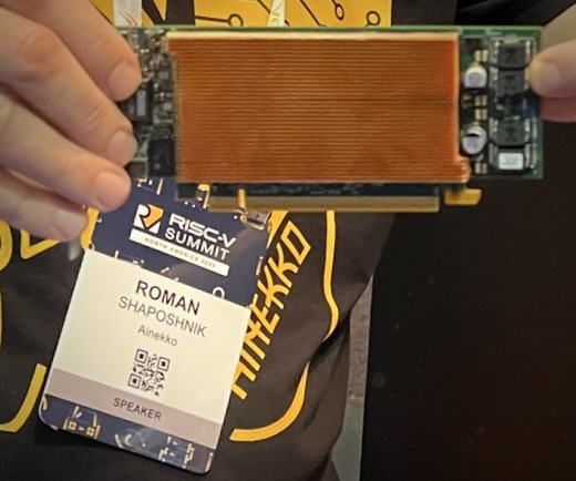
Overall, the minion cores look like nice little CPU cores - hopefully I'll be able to get my hands on some to play with soon (thankfully AINekko understand the importance of getting cards out for developers to play around with, but hardware takes time). This will allow me to explore my unanswered questions, such as:
- What clock speed are the minions running at? I think Esperanto's original goal was 1 Ghz, but reality might be more like 600 Mhz.
- Are "local" versus "global" atomics merely a performance optimisation, or are the "local" atomics actually non-coherent in some way?
- How good are these cores at hiding latency? Contemporary GPUs can round-robin between 16 warps in each warp scheduler, whereas minions can only round-robin between 2 threads.
- Can we run Linux on a 1056C / 2112T machine?